STM32: Урок 4 — GPIO
 GPIO (General Purpose Input-Output) — это выводы общего назначения, ноги микроконтроллера, доступные для прямого управления. Это обычно довольно дефицитный ресурс во многих популярных МК, но с STM32 эта проблема теряет актуальность: в самом мелком корпусе (LQFP48) доступно 37 GPIO, а в самом большом (LQFP176) — 140 GPIO. И всё это богатство ещё и настраивается вдоль и поперёк. Но, обо всём по порядку.
Для начала откроем руководство по STM32F100xx и взглянем на схему вывода порта:
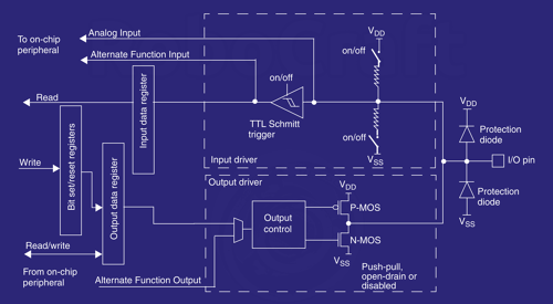
Сами МК питаются 3.3 В, но до сих пор ещё активно используются 5-вольтовые микросхемы и логика, а их нужно как-то подключать. Поэтому в STM32 большинство выводов «толерантны» к 5 В — уж не знаю, как ещё перевести термин «5 V tolerant». То есть, они могут принимать на вход 5 В без какой-либо угрозы их здоровью.
Толерантный пин отличается от обычного только тем, что у него верхний защитный диод подключён к Vdd_ft вместо Vdd. Из этой схемы становится понятно, что хоть выводы и толерантны к 5 В на вход, но вот выдавать 5 В на выход не могут — тут уже нужен транзистор. Если нужно получить логическую единичку, то это не проблема — 3.3 В вполне распознаются 5-вольтовой логикой как 1, но если нужно именно 5 В, то есть решение — режим Open-drain у GPIO.
Всего у STM32F10x режимов GPIO имеется 8.
Выход общего назначения:
- Push-pull, стандартный выход: выставляешь 0 в выходном регистре — получаешь низкий уровень на выходе, выставляешь 1 — получаешь высокий.
- Open-drain (открытый сток, аналог открытого коллектора): вывод подключен к стоку N-MOS полевика в то время, как P-MOS полевик заперт, что позволяет управлять нагрузкой с большим напряжением, чем Vdd (3.3 В). Кому там нужно 5 В на выход? Ниже я расскажу, как их получить.
Выход с альтернативной функцией (для периферии типа SPI, UART):
- Push-pull
- Open-drain
- Analog, аналоговый высокоимпендансный: подтягивающие резисторы и триггер Шмитта отключены. Используется при работе с АЦП.
- Floating, обычный высокоимпендансный: подтягивающие резисторы отключены, триггер Шмитта включен.
- Pull-up, вход с подтяжкой к питанию.
- Pull-down, вход с прижатием у к «земле».
Как водится, линии GPIO объединены в порты, в STM32 — по 16 линий, поэтому нумеруются они с 0 по 15: PA0, PA1 .. PA15 — это линии порта A, например. Линии порта управляются программно с помощью нескольких регистров.
GPIOx_CRL и GPIOx_CRH — регистры конфигурации, содержат настройки режима (вход/выход) и частоты GPIO. Доступны на чтение и запись.
GPIOx_IDR и GPIOx_ODR — входной и выходной регистры: в первом хранится считанное со входов порта значение, во второй записывается новое состояние выводов. GPIOx_IDR доступен только на чтение, а GPIOx_ODR — на чтение и запись.
GPIOx_BSRR и GPIOx_BRR — регистры атомарного изменения битов в GPIOx_ODR.
Обычно, если нужно установить бит в регистре периферии, то его сначала нужно прочитать, потом применить побитовое ‘ИЛИ’ к считанному значению и битовой маске, после чего записать новое значение назад в регистр. То же и со сбросом битов, только маску нужно инвертировать и применить побитовое ‘И’. А вот запись значений в GPIOx_BSRR и GPIOx_BRR изменяет только те биты выходного регистра, которые были установлены в единицу, притом происходит это за 1 такт, так что прерывание не сможет ворваться и всё испортить. Проиллюстрирую кодом:
Оба регистра доступны только на запись.
Всё это я рассказал для общего развития, а мы пока абстрагируемся от этих деталей, и будем всё делать через библиотеку SPL — с регистрами возится на данном этапе не резон.
В структуре GPIO_InitTypeDef из SPL, которую мы использовали в предыдущем уроке для инициализации GPIO, за режим отвечает поле GPIO_Mode, а константы для его заполнения имеют следующие имена:
- GPIO_Mode_Out_PP — выход push-pull
- GPIO_Mode_Out_OD — выход open-drain
- GPIO_Mode_AF_PP — альтернативная функция, push-pull
- GPIO_Mode_AF_OD — альтернативная функция, open-drain
- GPIO_Mode_AIN — аналоговый высокоимпендансный вход
- GPIO_Mode_IN_FLOATING — высокоимпендансный
- GPIO_Mode_IPU — вход с подтяжкой к питанию
- GPIO_Mode_IPD — вход с прижатием к земле
Подсмотреть это и многое другое можно в заголовочном файле stm32f10x_gpio.h, а в руководстве можно узреть ещё много интересного, включая детальные описания режимов и таблицу с описанием режимов GPIO для разной периферии — UART, SPI, I2C и др.
Пример инициализации GPIO для модуля USART1 и самого модуля на STM32VLDiscovery:
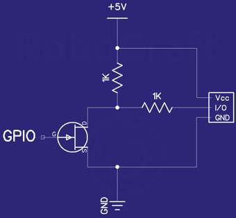
Что касается режима Open-drain, тут всё не так прямолинейно, как с другими режимами. Так как устройство, которым предполагается управлять, подключено к открытому стоку, нужно чуть более сложное соединение, чем обычно, а управление будет инверсное: выставляешь выход в 1 — ток с верхнего резистора идёт на землю, устройство видит на линии 0; выставляешь 0 — полевик запирается, ток идёт на устройство, на линии уровень 1.
Разработчики STM32 также позаботились об энергопотреблении и о снижении уровня помех, предусмотрев настройку частоты: по сути, входной и в ыходной регистры GPIO тактируются от отдельного источника, что позволяет задать свою частоту каждой ножке МК. Для STM32F10x доступны 3 частоты, которые представлены константами:
- GPIO_Speed_10MHz
- GPIO_Speed_2MHz
- GPIO_Speed_50MHz
Разумеется, частота GPIO не должна превышать частоту ядра (:
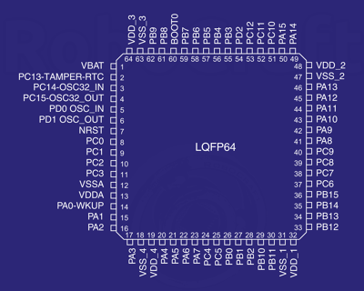
Ещё одна и интересная функция — переназначение выводов. Она позволяет переназначить выводы периферии с обычных на альтернативные, тоже фиксированные — впрочем, это не умаляет ценности данной функции: например, для USART1 можно переназначить TX с PA9 на PB6, а RX с PA10 на PB7. Если взглянуть на распиновку МК, можно увидеть, что обычные и альтернативные выводы находятся на разных сторонах кристалла, так что в разводке платы это в любом случае поможет:
А включается переназначение вот так:
Если вы два часа разводили двустороннюю плату, а потом обнаружили, что не можете развести какую-то сторону без огромной тучи переходов и перемычек, возможно, что функция переназначения выводов спасёт вашу клавиатуру от нелепой смерти под кулаком.
Есть у GPIO и довольно диковинная функция — блокирование выводов. Я так и не понял, зачем она может понадобится, но суть такова: можно заблокировать изменение состояния любого GPIO до следующей перезагрузки МК. Активируется тоже несложно:
Несколько слов об электрических характеристиках
В даташите по STM32F100xx встречаются рекомендации подключать не более 20 выводов с отдачей 8 мА через каждый или не более 8 выводов с 20 мА, но практически нереально найти информацию по максимальному току на вывод. Но есть таблица, где приведена максимальная рассеиваемая мощность для МК целиком, причём для разных корпусов эта мощность разная. Например, для LQFP64, в котором идёт STM32F100RBT6B на STM32VLDiscovery, эта мощность равна 444 мВт, что при напряжении питания 3.3 В даёт силу тока
134 мА. В другой таблице указано, что максимальный ток, потребляемый МК в режиме выполнения кода со всей включенной периферией при 100℃, составляет 15.7 мА. Итого имеем 134 — 15.7 = 118.3 мА на все выходы. Это максимальный ток, который может пропустить через себя МК, что немного расходится с рекомендациями. Впрочем, питать что-либо кроме светодиодов от MК в любом случае — плохая идея, а 118.3 мА хватит на пару-тройку десятков обычных светодиодов, которые при номинальном токе в 20 мА выжигают глаза, а при 1 мА вполне годятся в индикаторы.
Overview
There are not many people who can completely understand the internal structure and various modes of the GPIO (General Purpose Input and Output) of the processor. Recently, a lot of information about this part has been searched on Baidu, and many of the questions are not uniform. . This article will list all the issues involved in IO as much as possible, explain clearly the questions with clear answers, and raise questions for those who still have questions for discussion.
In a nutshell, the functional modes of IO can be roughly divided into three categories: input, output, and input and output.Among them, as the basic input IO, it is relatively simple, and the main knowledge involved is the high-impedance state. As the output IO, compared with the input, the working mode mainly has Open Drain mode and Push-Pull. Mode, this part involves more knowledge points; for input and output IO, the easy to be confused is the difference between quasi-bidirectional and bidirectional ports.
The details of each mode are described in order in this order.
Input IO
The input IO mentioned here refers to only the input and does not have the output function. At this point, the requirement for the input pin is high resistance (high resistance and tristate are the same concept). The types of basic input circuits can be broadly classified into three categories: basic input IO circuits, Schmitt trigger input circuits, and weak pull-up input circuits.
Start with the most basic basic input IO circuit, the circuit shown in Figure 1.

The buffer U1 therein is a tristate buffer having a control input and having high impedance characteristics. In layman’s terms, this buffer is high-impedance externally. It is equivalent to the fact that the physical pin is completely isolated from the internal bus when the control input is not enabled, and the internal circuit is not affected at all. The function of the control input is to issue an operation command to read the Pin state. The process is shown in Figure 2.

One disadvantage of this basic circuit is that jitter occurs when reading the edge of an external signal, as shown in the following figure.

Therefore, the Schmitt trigger input circuit solves the above-mentioned problem of jitter, and the signal after passing through the Schmitt trigger is as shown in FIG.

Another problem with the input circuit is that when the input pin is left floating, is the level detected at the input high or low? When the input signal is not driven, that is, floating, any noise on the input pin changes the level detected at the input, as shown in Figure 5.

To solve this problem, a weak pull-up resistor can be added to the input pin, as shown in Figure 6.

Thus, when the input pin is left floating, it will be pulled high by RP and there will be a certain state on the internal bus.
But this structure has certain problems. The first obvious point is that when the input pin is left floating, it reads 1 and when the input pin is driven high, it reads 1 and only reads when the input pin is driven low. It is 0. That is, the way to read 1 is to "read non-zero".
Another problem is that the circuit is not high-impedance externally, and in some sense is also outputting outward. When the external driving circuit is different, an erroneous detection result may occur. For example, the external driving circuit is a structure as shown in FIG. 7, in which a high level or a low level can be output by K to a different end.

If the circuit shown in Figure 7 is output low, it is connected to an input pin with a weak pull-up resistor. The structure is as follows.

According to Ohm’s law, the level at the test point is Therefore, the input signal measured by the CPU is high, and the external drive circuit expects the output level to be low. The reason for this error is that the input circuit of this structure is not really high impedance, or the input IO is actually output, and it affects the external input circuit.
The occurrence of this situation also shows that the signal is transmitted in two stages before and after, why the output impedance is small and the input impedance is large. In this example, the output impedance of the peripheral driver circuit is very large, reaching 100Kohm; and the impedance at the input is not large enough, only 10Kohm, so there is a problem. If the input impedance at the input is truly high impedance (infinity), as shown below, there will be no problems.

The input circuit with weak pull-up mentioned above is the case of the quasi-bidirectional port mentioned in the following sections.
Output IO
The two main modes of the IO output circuit are Push-Pull Output and Open Drain Output.
Push-Pull Output
The structure of the push-pull output is controlled by two transistors or MOS tubes with complementary signals. The two tubes are always kept one off and the other is on. As shown in Figure 10.

The biggest feature of the push-pull output is that it can truly output high level and low level, and has driving capability at both levels.
Supplementary note: The so-called driving ability refers to the ability to output current. For driving large loads (ie, the smaller the internal resistance of the load, the larger the load), for example, the IO output is 5V, and the internal resistance of the load is 10 ohms. Therefore, according to Ohm’s law, the current on the load can be normally 0.5A (calculated) The power is 2.5W). Obviously, the general IO cannot have such a large driving capability, that is, there is no way to output such a large current. The result is that the output voltage will be pulled down and will not reach the nominal 5V.
Of course, if only the digital signal is transmitted, the input impedance of the next stage is theoretically high impedance, that is, only the voltage needs to be transmitted, there is basically no current, and there is no power, so that a large driving capability is not required.
For the push-pull output, the current flow when the output is high or low is shown in Figure 11. Therefore, compared with the open-drain output described later, the driving ability at the output high level is much stronger.

However, one disadvantage of the push-pull output is that if the two push-pull output structures are connected together, one output is high, that is, the upper MOS is turned on, and the lower MOS is turned on; while the other output is low, that is, the upper The MOS is closed and the lower MOS is turned on. The current flows directly from the VCC of the first pin through the upper MOS and through the lower MOS of the second pin to GND. The resistance on the entire path is small, and a short circuit may occur, which may cause damage to the port.This is also the reason why the push-pull output cannot achieve "line and".
Open Drain Output
It is often said that the open-drain output is the opposite of the push-pull output. The most common difference between the open-drain output and the push-pull output is that the open-drain output cannot truly output a high level, that is, there is no driving capability at a high level, and it is necessary to use an external The pull-up resistor completes the external drive. The following is an explanation of the internal structure and principle of why there is no driving capability when the open-drain output is high, and further compares the difference with the push-pull output.
First, we need to introduce some open-drain output and open-collector output. The principle and characteristics of these two outputs are basically similar. The difference is that one uses a MOS tube, where "drain" refers to the drain of the MOS tube; the other uses a triode, where the "set" refers to the triode collector. Both of these are actually output modes corresponding to the push-pull output. Since the MOS tube is used more often, the word "open-drain output" is often used instead of the open-drain output and the open-collector output.
The introduction begins with the open collector output, and the schematic circuit junction is shown in Figure 12.

The circuit on the left side of Figure 12 is the most basic circuit for the open-collector (OC) output. When the input is high, the NPN transistor is turned on, the Output is pulled to GND, and the output is low. When the input is low, the NPN transistor Closed, Output is equivalent to an open circuit (output high impedance). Output high impedance at high level (What are the meanings of high resistance, tristate, and floating? High resistance and dangling are not a meaning), there is no driving capability at this time. This is the biggest feature of open drain and open collector output. How to use this feature to complete various functions will be introduced later. Although this circuit completes the function of the open collector output, it will appear that the input is high and the output is low; the input is low and the output is high.
In the circuit on the right side of Figure 12, a triode is used to complete the "inversion". When the input is high, the first transistor is turned on, and the input of the second transistor is pulled to GND, so the second transistor is closed and the output is high impedance; when the input is low, the first The transistor is closed, at which point the input of the second transistor is pulled high by the pull-up resistor, so the second transistor is turned on and the output is pulled to GND. Thus, the input and output of this circuit are in phase.
Next, the circuit for open-drain output is shown, as shown in Figure 13. The principle is basically the same as the open collector output, except that the triode is replaced by MOS.

Then talk about the characteristics of open-drain and open-collector output and their applications. Since the two are similar, if there is no special explanation in the following, open-drain and open-collector output circuits are indicated by open-drain.
The main characteristic of the open-drain output is that the high level has no driving capability, and an external pull-up resistor is required to actually output a high level. The circuit is shown in FIG.

Figure 14
When the MOS transistor is closed, the open-drain output circuit outputs a high level, and when connected to the load, the current flows from the external power supply, flows through the pull-up resistor RPU, flows into the load, and finally enters GND.
An obvious advantage of this feature of the open-drain output is that the level of the output can be easily adjusted because the output level is completely determined by the power supply level to which the pull-up resistor is connected. Therefore, where level shifting is required, it is very suitable to use the open drain output.
Another benefit of this feature of open-drain output is that it can implement the "line and" function. The so-called "line and" means that multiple signal lines are directly connected together, only when all When the signals are all high, the combined bus is high; as long as any one or more signals are low, the bus is low. The push-pull output will not work. If the high level and the low level are connected together, current backflow will occur and the device will be damaged.
Difference between push-pull and open-drain output

Figure 15
Two-way IO
Many processor pins can be configured as bidirectional ports. The requirement for bidirectional ports is to both output the signal and read back the external signal input. To achieve these two points at the same time is somewhat difficult in principle. First, let’s start with the internal structure of the open-drain output IO port of the processor, as shown in Figure 16.

The structure is based on Figure 13, with an FF added before the transistor for the purpose of controlling the timing of the output signal. A more common application is when multiple IOs are used as a bus, each pin on the bus is required to simultaneously output data.
For the open-drain output structure, the output Q terminal of the FF is connected to the drive buffer, so that the read operation is read not by the state of the external pin, but by the state of its own output.
Two-way open drain IO
However, the structure of Fig. 16 is slightly modified. As shown in Fig. 17, the structure is called a bidirectional open drain IO structure. The change was to connect the input driver buffer to the PIN.

When the output of the structure is "1", T1 is turned off, and the pin presents a high resistance to the outside, and there is no problem as an input pin. However, if the structure outputs "0", T1 is turned on, and the pin is short-circuited to the ground, that is, no matter what signal is externally input, all of the U2 read back is low. Therefore, for such a structure, if it is required to be used as an input pin, it is necessary to output "1" to U1 to read the external pin data.
Quasi-bidirectional open drain IO
Quasi-bidirectional ports are also mentioned in many documents. In fact, the quasi-bidirectional port is a pull-up resistor added to the structure of Figure 17, as shown in Figure 18.

This structure has the following differences and differences compared to Figure 17:
When used as an input pin, you must also write "1" to U1 to achieve the purpose of disconnecting T1. So whether you need to write "1" in advance is not the difference between bidirectional IO and quasi-bidirectional IO. Both of them must be written "1" in advance when they are used as input ports.
When the bidirectional port is input as a true high-impedance state, and the quasi-bidirectional IO is used as an input port, the input impedance is not high-resistance, so there may be a problem as shown in Figure 8 of this figure. .
The quasi-bidirectional port reads the input state and defaults to high. That is, the method of judging the external input signal is "not low is high". That is, the structure can only accurately identify the external low level, and cannot distinguish between the dangling and the true high. So as long as the reading is not 0, the external is considered to be 1.
Push-pull output as bidirectional IO
If the output portion of the bidirectional port is a push-pull output structure, then all ports of the upper and lower tubes must be made high impedance as an input.
51 single-chip P0 port
In the discussion of the bidirectional port, the more complicated one is the P0 port of the 51 MCU. Here we discuss in detail the structure and working principle of the P0 port of 51 single-chip microcomputer.
The internal structure of the P0 port is shown in Figure 19.

The internal structure is complex and includes the following devices:
U1: AND gate. One input is connected to the control line and the other input is connected to this address/data signal. Due to the characteristics of the AND gate, when the control line is 1, the AND gate output is consistent with the level of the address/data signal; if the control line is 0, the output is constant. The control signal line then corresponds to the enable signal of the AND gate.
U2: Inverter, the output signal is the inverted signal of the address/data signal.
Both U3 and U6 are tristate buffers with control inputs and high impedance characteristics that act to present a high impedance state for the outside. The level of the external signal can be read into the data bus when the control is enabled.
U4: is the latch, the purpose is to control the time of the pin output signal.
U5: Analog switch that controls whether the input signal to V2 is from the Q non-output of latch U4 or from the output of inverter U2.
V1 and V2 are two MOS tubes, respectively.
After learning about the individual devices, I started to explain how working in each mode works:
When P0 is used for address/data lines:
When P0 is used as the address/data line, it is the address and data multiplexing bus. P0 needs to output the address and needs to read back the data signal.
When P0 needs to output address information, the control signal of U1 is 0, and the analog switch U5 is connected to the output of the U2 inverter. Therefore, when the signal transmitted from the address signal line is 1, the input signal output to V1 is "1" after the control line "1" is phased, and V1 is turned off. After the address signal "1" is inverted, the input to the V2 through the analog switch is "0", and V2 is turned on. Thus, as shown in Fig. 20, the pin outputs "0".

When the signal transmitted from the address signal line is 1, the input signal to V1 is "0" after the control line "1" is phased, and V1 is turned on. After the address signal "0" is inverted, the input to the V2 through the analog switch is "1", and V2 is turned off, so the situation is as shown in Fig. 21, and the pin outputs "1".

Therefore, when outputting as an address line, both MOS transistors V1 and V2 are used, which is a push-pull output.
When P0 outputs the lower 8-bit address information, it will become the data bus. At this time, the CPU operation is the control terminal output 0, the analog switch hits the Q non-terminal of the latch, and "1" is entered into the latch. ". Then Q non-output is 0, V2 is cut off. At the same time, the control line is 0 so that the AND gate output is 0 and V1 is turned off. Since both V1 and V2 are off, the pin is completely high impedance at the moment. As an input port, external data enters the internal bus through U6, as shown in Figure 22. (Equivalent to disconnecting all the two MOS transistors of the push-pull output.) At this time, since it exhibits high resistance, it is a true input pin. This explains why P0 is a true two-wire port.

When P0 is used for normal IO:
When P0 is used as a normal IO and as an output, the control signal is 0, so that V1 is always off. The analog switch is connected to the Q non-output. When used as an output, the input of the latch directly inputs 0 or 1. Q does not input the inverted signal to the input of V2. That is, when "0" is output, the V2 input terminal is "1", V2 is turned on, and the pin output is "0". When the output is "1", the V2 input terminal is "0", V2 is turned off, and the pin output is high impedance. . That is, when P0 operates in the normal IO mode, the output is an open-drain output, and there is no pull-up resistor inside.
When P0 is used as a normal IO and as an input, the control signal is 0, so that V1 is always off. The analog switch is connected to the Q non-output, and the CPU automatically writes 1 to the latch input. The V2 input is 0 and V2 is turned off. As before, as the address/data line, as the input, the two MOS tubes are all disconnected, and the pin is directly connected to the U6, which presents a high resistance to the outside. So it is also the real input pin.
In summary, P0 is true dual port IO no matter which mode it is working on.
P3 port of 51 single chip microcomputer
The internal structure of the other three ports of the 51 MCU is shown in Figure 23. Compared with P0, it is much simpler. There is no MOS tube at the top, and there is no option for address/data signals. As an output, it is an open-drain output with a pull-up resistor. When it is input, there is a pull-up resistor, so the input port is not high-resistance externally. This explains why P1 to P3 can only be quasi-bidirectional ports.
Микроконтроллер под микроскопом
Наверняка вы уже знаете, как устроен компьютер. Даже на бытовом уровне вы представляете, что такое память RAM и ROM. Также знаете, что информация в компьютере представляется в двоичной форме. Однако этих знаний нам недостаточно для того, чтобы начать работать с микроконтроллером.
Помимо уже упомянутых видов памяти и непосредственно самого процессорного ядра в микроконтроллер входит регулятор напряжения, генератор тактового сигнала, системная шина, различные контроллеры, блок системы прерываний, периферийные устройства и т.д.
Однако, первое, с чем нам придется ознакомиться – с особым видом памяти под названием «регистр».
Что такое регистр?
Регистр (англ. register) – это устройство, расположенное внутри ядра микроконтроллера (или процессора), для хранения n-разрядных двоичных данных и выполнения преобразований над ними. Скорость их работы очень высока. Регистр представляет собой упорядоченный набор триггеров, или переключателей (англ. trigger), способных принимать значение «0» (потенциал равен 0 вольт) или «1» (потенциал равен рабочему напряжению для внутренностей МК, в нашем случае это 1,8 вольта). Число триггеров n соответствует числу разрядов в слове. В свою очередь, машинное слово — платформозависимая величина, измеряемая в битах (или байтах) и равная разрядности регистров процессора и/или разрядности шины данных. Так, например, наш микроконтроллер является 32-разрядным, а это значит, что слово состоит из 32 бит (или из 4 байт). Специальные регистры — это часть RAM-памяти. Их функции определены производителем и не могут быть изменены. Все биты (триггеры) такого регистра подсоединены к определенным цепям внутри микроконтроллера, т. е. изменение состояния триггера напрямую влияет на работу микроконтроллера (отдельных его частей/цепей). Например, записав «0» в ячейку памяти регистра, отвечающего за порт ввода/вывода, вы определяете его функцию: будет он работать на вход (т. е. принимать сигналы) или на выход (т. е. посылать сигналы).
Так как мы будем использовать язык программирования Си, то будет правильно напомнить некоторые операции, которые позволят нам быстро и удобно настраивать необходимые биты в регистре. Первое, что стоит вспомнить – это операции побитового смещения. Допустим, нам нужно получить число 8. Мы уже знаем что 810 равно 10002. Таким образом, чтобы получить 8, нам всего-то нужно передвинуть в памяти «1» на три позиции влево. Сделать это можно так: